2020年4月24日 星期五

材料分析Part B-4-2 TEM/STEM影像

現代TEM/STEM系統有二大影像模式:TEM影像和STEM影像。TEM影像如圖B-24所示,包含明場(BF)像,暗場(DF)像,和高分辨(HRTEM)影像三種。前二種的分辨率在0.3 ~ 0.4 nm之間,倍率範圍從1000X 100KX之間;HRTEM影像的分辨率可達到約0.16 nm,倍率範圍從100KX 1000KX之間。STEM影像有明場像,環形暗場(ADF)像,高角度環形暗場(HAADF)像,高分辨(HRSTEM)影像(通常倍率大於5MX)等幾種。STEM影像的好處是影像可以自由旋轉,對於半導體元件的影像,很容易將基板和薄膜的界面調成水平方向。2015年後的TEM如果安裝4K x 4KCCDCMOS數位相機,只擷取2K x 2K的影像,也有同樣的功能。
There two main types of images, TEM images and STEM images, for current TEM/STEM systems. TEM images include bright-field (BF) images, dark-field (DF) images, and high resolution TEM (HRTEM) images, as shown in Fig. B-24. The routine magnification for both BF/DF images falls in the range of 1000X to 100KX, the best resolution of BF/DF images is about 0.3 to 0.4 nm. The magnification used for HRTEM images is from 100KX to 1000KX, and the resolution approaches 0.16 nm. STEM images include bright-field images, annual dark field (ADF) images, and high angle annual dark field (HAADF) images, high resolution STEM (HRSTEM) images (> 5 MX). The advantage of STEM images is free to rotate images, so all STEM images of semiconductor devices can easily be set all interface running horizontally. For TEMs manufactured after 2015 and equipped with a 4K x 4K CCD (or CMOS) camera, all TEM images can do the same rotation if only images of 2K x 2K taken.


B-24. TEM模式下的典型影像。(a)明場像;(b)中央暗場像;(c)高分辨影像;(d)和局部放大高分辨影像。

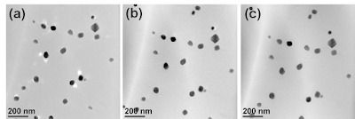
嚴格定義的TEM明場像是使用最小的物鏡光圈,只讓透射電子束通過成像,但是此種影像對比過於強烈,影像非黑即白缺少灰階變化,所以除非分析晶體缺陷,很少使用此類型的明場像,而是用大一點的物鏡光圈,包含部分第一階的繞射電子束,緩和影像對比,在影像中增加一些灰階層次。在這類型的TEM明場像,物鏡光圈除了調整對比外,也有減少物鏡球面像差的功能,如圖B-25所示,在無物鏡光圈時,某些黑色顆粒的旁邊會有一形狀大小相同的顆粒,放入100 um的物鏡光圈後,大部分顆粒消失,只剩下一,二顆微粒的側緣有亮線,這是物鏡球面像差造成的影像,所以在使用30 um物鏡光圈的影像內這些假像完全消失。根據經驗,分析奈米材料時,必須使用60微米以下的物鏡光圈,才能得到清晰且沒有亮點假象的奈米相TEM明場像。
The strict BF image means those images using the smallest objective aperture to block all diffracted beams and allowing only the transmitted beam to pass to form the image. The contrast of this kind of BF images is too high, absent of grey levels. We use this kind of BF image to analyze crystal defects only. We usually use a larger objective aperture to include several diffracted beams as well as the transmitted beam to form BF images with tones of grey. Besides changing the contrast of images, the objective aperture can reduce spherical aberration, as illustrated in Fig. B-25. Some particles in the BF image without objective aperture are coupled with a “bright shadow”, all of these “bright shadow” disappear when a 100um objective aperture is used, butl a few of particles with bright lines aside are still observed. There is no bright line observed at any particle when a 30um objective aperture is used. According to experience, it is better to use objective aperture not larger than 60um to minimize the effect of spherical aberration to obtain clear BF images of nano phases, especially nano wires.

B-25. TEM明場像。(a)無物鏡光圈;(b)物鏡光圈 = 100 um(c)物鏡光圈 = 30 um


一般的TEM暗場像一定使用小於30 um的物鏡光圈擋住透射電子束和其他的繞射電子束,只讓某一特定的繞射電子束通過成像。而且此繞射電子束必須傾轉到光軸上,形成中央暗場(CDF)像,暗場像上的的球面像差效應最小,影像才會清楚,如圖B-26所示,只有在中央暗場像才看得到鎢矽化物內的疊差,而偏離光軸的暗場像因球面像差之故,分辨率不足,無法解析細微的結構。
Generally, a TEM DF image uses an objective aperture < 30um to block transmitted beam and other diffracted beams, only allow one specific diffraction beam to pass through to form a DF image. This selected diffracted beam should be tilted to go along the optical axis to for a center dark field (CDF) image that minimize the effect of spherical aberration in the DF image, as shown in Fig. B-26. The tiny structure, such as a stacking fault in the tungsten silicide, can only be observed in the CDF image, but not in the DF image that has significant spherical aberration resulted from using an off-axis diffracted beam.


B-26. TEM模式下的明場像(a),對應的暗場像(b),與中央暗場像(c)


可以得到前述二種影像的試片和機台條件,不一定可以得到HRTEM影像。要得到足夠清晰的HRTEM影像,下列幾個條件必須同時滿足。(1)試片必須是晶體而且夠薄,而且因試片製備造成的表面損傷層要更薄;(2)晶體的低指數晶軸(low index zone axis)要能夠被傾轉至和電子束平行;(3)TEM物鏡散光必須調整至接近零的狀態;(4)適當的物鏡欠焦(under focus)
It is easy to acquire both BF and DF images when a TEM specimen is inserted, but it requires some special conditions to get good HRTEM images. First, the TEM specimen must be a crystal and thin enough with a very thin damaged layers on the surfaces. Second, the low index zone axis of the crystal has to be tilted parallel to the TEM optical axis. Third, TEM must be well aligned especially the astigmatism of the objective lens. Fourth, optimum under focus has to be used.

STEM明場像可用STEM BF影像偵測器攝取,也可用環狀影像偵測器搭配大於3米的相機長度攝取。整體來說,STEM明場像和TEM明場像很類似,但是因試片彎曲造成的條紋,在STEM明場像中可以被緩和許多。當相機長度逐漸減小時,環狀影像偵測器內收集角逐漸變大,透射電子束直接穿過中間中空區域,只有繞射電子束形成影像,是為環形暗場像。當相機長度變得很小時,環狀影像偵測器內收集角變得很大,環狀影像偵測器只收集到被彈性散射到高角度的彈性散射電子,此時攝取到的影像是為高角度環形暗場像。相機長度,內收集角,和收集訊號種類的關係說明於圖B-27中。
STEM BF images can be acquired by an annual dark filed (ADF) detector as well as a STEM BF detector. When a ADF detector is used to acquire STEM BF images, a large camera length (CL) has to be used. STEM BF images look similarly to corresponding TEM BF images. However, many bend contour fringes in TEM BF images can be eliminated in STEM BF images. The inner collection angle of the ADF detector increases gradually when the CL becomes small and small. The ADF detector then collected signals in diffracted beams only, so we call this kind of images to be annual dark field images. The inner collection angle of the ADF becomes very large when the CL becomes very small. Only those electrons elastically scattered to high angles are collected at this moment, STEM images at these conditions are called high angle annual dark field (HAADF) images. Relationships among CLs, inner collection angles, and signals are described in Fig. B-27.  


B-27. STEM模式下相機長度(CL),內收集角(θin),和收集訊號種類的關係。

2020年4月19日 星期日

材料分析Part B-4 穿透式電子顯微鏡(TEM) -B-4-1 TEM簡介

將圖B-9中試片的厚度降至150奈米以下,再將入射電子的加速電壓增至100 KV以上,則絕大多數的入射電子會穿過試片。這些穿過試片的電子可以初步劃分為「未被未被散射電子」,「彈性散射電子」,「非彈性散射電子」三大類,如圖B-20所示。穿透式電子顯微鏡的訊號偵測器接收這些電子後,形成繞射圖案、影像、電子能量損失能譜等資料,再加上背向的X光訊號,組成一套可同時分析奈米微區的結構、組成、晶相等的材料分析技術。
If the specimen thickness in Fig. B-9 is reduced to thinner than 150 nm, and the acceleration voltage is increased up to 100 KV and higher, most of incident electrons will penetrate the specimen. Electrons through the specimen are divided into three groups: un-scattered electrons, elastically scattered electron, and inelastically scattered, as shown in Fig. B-20. All these signals are then acquired by detectors in TEM to be data of diffraction patterns, images, electron energy loss spectra as well as characteristic X-ray emitting from the other side. This is a materials analysis technology being able to resolve the microstructure/composition/crystallography of a volume of nano scale simultaneously. 


B-20. 高能電子射入薄片試片後產生各種電子訊號的示意圖。


B-21展示一傳統型式TEM/STEM的外形和基本結構示意圖,以及上述各種訊號形成的相對位置。電子束穿過薄片試片後,先在物鏡的後聚焦面處形成電子繞射圖案,然後在第一成像面形成倒立放大實像,電子能量損失能譜儀(EELS)安裝在傳統相機室的下方,接收多數穿透過試片的電子,並依能量損失量線性排列成電子能量損失能譜,能量散佈能譜儀(EDS)則安裝在試片斜上方,接收入射電子撞擊試片後產生的特性X光。
A traditional TEM/STEM and its schematic configuration are shown in Fig. B21. Locations of typical TEM/STEM data generated are pointed out too. After penetrating the foil specimen, high-energy electrons form a diffraction pattern at the objective back focal plane, a magnified image at the first image plane. An EELS is installed at the bottom of the TEM column to collect most electrons through the specimen. An EDS is equipped at diagonally above the specimen to collect characteristic X-ray emitting from the specimen.


B-21. 傳統TEM的外形、基本結構、典型訊息及其產生的位置。


以前TEM依其性能區分成三大類型:傳統TEM(CTEM),高分辨TEM(HRTEM),分析式TEM(AEM)CTEM的最佳影像分辨率(解析度)略大於0.2 nm,其物鏡間隙較大,試片的傾轉角度可達45度,可以從數個特定晶向分析同一個晶體;HRTEM的最佳分辨率(解析度)小於0.2 nm,但其物鏡間隙較小,試片的傾轉角度約只有15度;AEM則是有STEM模式,電子束一般可達2 nm,使用場效電子鎗的STEM可達1 nm,加裝EDSEELS或二者都有以便進行成份分析。三種TEM機型對應的主要操作模式如圖B-22所示。1995年後,因為日漸精密的機械加工與電腦輔助系統的引入,三類TEM之間的疇界逐漸被打破。現在的TEM都是使用場效電子鎗,影像最佳分辨率(解析度)達到0.16 nm,同時有STEM模式,而且STEM的影像解析度可達0.2 nm。二種模式的切換只是按鈕動作,加上一些微調即可。圖B-23顯示現代TEM機台擁有的功能,其中新型空影像最早於1992年出現在Zeiss 912 TEMZeiss退出TEM市場後,PhilipTecnai系列繼承此成像功能,而後FEI-Philip到目前的Thermo-FEI的所有TEM/STEM都有此成像功能。另外上有些TEM使用特別設計的物鏡和試片承載台,可進行臨場(in-situ)實驗。而加上球面像差矯正器的TEM/STEM,影像分辨率和解析度都可優於0.1 nm,只是價格相對高許多。
TEMs were used to divided into three groups: conventional TEM (CTEM), high-resolution TEM (HRTEM), and analytic TEM (AEM). The gap of the pole piece of CTEMs is large enough to tilt the specimen up to 45 degree, so a special crystal can be analyzed from several low index zone axes. The image resolution of CTEMs is a little larger than 0.2 nm. HRTEMs had a smaller pole-piece gap, tilting angle is usually limited to be 15 degree, and has an image resolution approaching to 0.18 nm. AEMs were used for composition analysis by EDS or EELS or both in STEM mode. Its probe size was about 2 nm for a LaB6 emitter and 1 nm for FEG type. After 1995, most of TEMs are FEG type with image resolution better than 0.2 nm and coupled with STEM mode with probe size smaller than 0.2 nm due to the progress in precision machining and the aid of personal computer in operation system. Now, one TEM/STEM has functions shown in Fig. B-23. New type hollow cone showed up in Zeiss 912 in 1992, and Philips Tecnai series (then FEI-Philips and Thermo-FEI TEM/STEM) after Zeiss withdrawing from the TEM market. Some TEM/STEM can do in-situ experiment with special a designed objective chamber and specimen holders. The image resolution as well as electron probe size can be improved to beyond 0.1 nm when an objective and a C2 spherical correctors are equipped. However, the price goes up very much.


B-22. 傳統TEM機型的分類,與其主要的操作模式。


B-23. 現代TEM/STEM經常性操作模式。


2020年4月16日 星期四

材料分析Part B-3 聚焦離子束(FIB)

聚焦離子束(focus ion beam, FIB)原來用於半導體元件的線路修補,利用鎵離子束轟擊功能有誤的半導體元件的局部線路,將其切割,再利用鎵離子束加強化學氣相沈積法(ion beam enhanced CVD),在該局部區域沈積介電層(通常使用二氧化矽),最後仍用鎵離子束加強化學氣相沈積法跨接金屬線形成新迴路。
Focus ion beam (FIB) was designed to do circuit repair. Parts of metal lines in a semiconductor device with improper function are cut by FIB with its Ga+ ion bombardment. These removed parts are then filled with dielectric material (SiO2 usually) by using ion beam enhanced CVD (chemical vapor deposition). A new circuit is then re-built by connecting some metal lines by ion beam enhanced CVD metal.

由於FIB具有精準缺割的功能,半導體元件的橫截面分析可直接臨場進行,不用取出研磨拋光後再放回SEM進行分析,節省許多樣品製備的時間。雖然鎵離子掃描樣品時可產生二次電子,形成二次電子影像供分析樣品結構,但是由於高能離子的轟擊作用,二次電子影像看到的顯微結構已經是過去式的顯微結構。為了降低輻射損傷,盡量看到並同時保留樣品的現時真實結構,新一代的FIB加裝電子鎗,用電子束掃描成像。這種同時有離子鎗和電子鎗的FIB稱為雙束聚焦離子束(dual beam FIB),其結構示意圖如圖B-16所示。離子束和試片表面的法線平行,電子束則和法線傾斜一個角度,目前通常是52度。
Due to its accurate cutting function, FIB can be used to analyze the cross-section structure of semiconductor devices by collecting secondary electrons excited by Ga+ ions to form SEIs. However, the structure is damaged after ion beam scanning, and the secondary electron image shows the past structure instead of current structure. An electron gun emitting electron beam to scan the sample was then added to the new generation FIB. This type of FIB is called dual beam FIB, schematically shown in Fig. B-16. Ion beam is parallel to the normal of the specimen, and electron beam usually tilts 52 degree away from the normal.


B-16. 雙束聚焦離子束結構示意圖。(Ref : DM of FEI)
現在新型的雙束FIB電子束分析,除了電子束不垂直試片表面外,其他和影像和SEM幾乎完全一樣,也有二次電子和反射電子二種模式。在FIBSEIsBEIs上水平距離(x)的量測也可以用影像上的標尺比對,但是垂直距離(y)則必須在FIB內,直接用影像軟體量測,或者要經過角度投影換算,如圖B-17所示。典型半導體元件的雙束FIB二次電子影像如圖B-18所示。
Current dual beam FIB can perform materials analysis by using SEI and BEI as SEMs do. The only difference is that the electron is parallel to the normal of the specimen surface in SEM but it tilts 52 degree away from the normal in FIB. Under such condition, only the horizontal distance can be measured by using the micro bar in the image, any vertical distance has to be measured by the built-in program or multiply a factor as illustrated in Fig. B-17. A typical FIB secondary electron image of a semiconductor device is shown in Fig. B-18.


B-17. 雙束聚焦離子束中電子影像y方向距離的修正。


B-18. 典型半導體元件的雙束FIB二次電子影像。


雙束FIB除可用二次電子和反射電子做影像分析外,也可加裝EDS做成份分析,加上本身具有臨場切割的能力,已取代一部分的SEM市場。雙束FIB另一大市場是半導體元件的TEM試片製備,在未來的章節再詳細討論。
Besides image analysis by using SE and BE, FIB is also able to perform composition analysis by attaching an EDS system. SEM has been replaced by FIB in some laboratories in many ways, because the latter has the ability of in-situ cutting as well as materials analysis. Another major application of FIB is to make TEM specimens of semiconductor devices. It will be discussed in detail later.

FIB 切割實心樣品做橫截面分析時,除了因離子轟擊造成的表面損傷外,沒有其他明顯的問體。但是如果切有中空的樣品時,經常會因再沈積的作用,在中空處上緣多出一層材料出來,如圖B-19示意圖所示。
There is no obvious problem in cutting solid samples, excluding surface damage due to ion beam bombardment. But there will be a significant extra layer at top and sides for a hollow structure as shown in Fig. B-19.

B-19. 中空結構的元件在FIB切割過程中,會在空孔的上緣和側邊多出一層薄膜(a)without FIB cutting(b) with FIB cutting

2020年4月12日 星期日

材料分析Part B-2-4 加速電壓對SEM影像的影響

二次電子和反射電子穿入試片的深度(B-9中的hShB)SEM的加速電壓與試片的組成元素有關。同樣的材質,加速電壓愈大,訊號來自愈深層,如圖B-14所示;同樣的加速電壓,試片組成元素的原子序愈大,電子束穿透能力愈低,訊號來自較淺層的區域。圖B-15顯示一組不同加速電壓的雲母片二次電子影像。圖B-15 (a)的加速電壓為15 KV,圖B-15 (b)的加速電壓為3 KV。在15 KV的加速電壓下,雲母片呈半透明狀態;而在3 KV的加速電壓下,雲母片表面的微粒清晰可見。改變加速電壓,探索試片表面至深層的不同結構是SEM操作者必備的進階技術。
The real depth of SE and BE emitting from the specimen depends on the accelerated voltage and the composition of the specimen. Signals are from deeper regions when higher acceleration voltage is used for a specified specimen, as shown in Fig. B-14. For a specimen consisted of heavy elements (high atomic number atoms), the ability of penetration of the high energy electrons becomes smaller and signals emit from shallower regions. Fig. B-15 shows two SEM SEI of mica slices by 15 KV and 3 KV acceleration voltages respectively. Mica slices look semitransparent in the SEI of 15 KV, and particles on mica surfaces are clearly visible in the SEI of 3 KV. A skill SEM operator knows how to acquire the structure of different level by using different acceleration voltage.


B-14. 加速電壓對電子束穿透力與訊號產生範圍的影響。(Ref: Practical Scanning Electron Microscopy, edited by J. I. Goldstein, etc., 3rd edition, New York  (1977).)


B-15. 雲母片SEM二次電子影像。(a)Vacc = 15 KV(b) Vacc = 3 KV(感謝工研院工材所陳世昌先生提供,1996)

2020年4月9日 星期四

材料分析Part B-2-3 SEM影像對比機構

SEM影像主要分成二大類:二次電子影像和反射電子影像。圖B-9指出二次電子影像來自較淺層的區域,約從上表面起到下方100奈米的深度,有較佳的解析度;反射電子則來自上表面至下方數微米的區域,因為電子束擴展效應(beam broadening),產生訊號的直徑可能10倍電子束大小,所以在同樣的加速電壓條件下解析度比二次電子影像差。應用這種來自不同深層的影像特性,在半導體元件的某些類型失效分析上有其獨特的效果。半導體元件的失效如果發生在某一層的金屬線路上,在分析過程中,其上層的金屬層必須先磨除,但是失效金屬層上方的金屬間介電層(IMD)卻必須保留。此時BEI影像才能看清楚失效金屬層因製程缺陷造成的損傷。
There two types of SEM images, SEI and BEI, used routinely. As shown in Fig. B-9, for an incident electron beam, SEI is formed by SE emitting from shallow region less than100 nm below the top surface and has better spatial resolution, while BEI is formed by BE emitting as deep as several micrometer , and from a volume with a diameter ten times larger than the electron beam due to the effect of beam broadening. From time to time, it is useful to use signals emitting from different depth in failure analysis of semiconductor devices. For example, if the failure occurred in a metal layer, all metal layers above it must be removed, while the IMD layer above it must be kept. BEI works well when deep feature is the point.


B-9. 高能電子射入塊材試片後產生二次電子和反射電子的示意圖。


二次電子的能量落在0 ~ 50電子伏特範圍,只能從較淺的表面層逸出,所以表面型態會影響二次電子的產生率,進而產生明暗對對比。二次電子影像的對比機構是表面型態對比(topography contrast),以圖B-10(a)解說,較易瞭解。對於同材質的試片,粗糙不平的表面,在二次電子影像中,會比光滑的表面亮。從黑白灰階影像明暗代表的意義,告訴我們粗糙不平的表面產生較多的二次電子。圖B-11解釋此結果的緣由,雖然整個水滴型的體積內都產生二次電子,但是只有在距離表面一定深度以內的二次電子才能逸出試片,也就是圖B-11中藍色區域的二次電子才能跑出試片成為有效的訊號。從圖B-11示意圖中明顯看出在不同幾何面的二次電子的產生率,九十度轉角的區域產生的二次電子最多。圖B-12是一典型含有九十度轉角結構的二次電子影像,每個九十度轉角結構都有一條亮線(紅色箭頭指處)
Since SE can emit from a depth less than 100 nm below the top surface, the morphology of the specimen surface will affect the yield of SE, then induce contrast in the image. Topography contrast dominate in SEI as shown in Fig. B-10(a). For the same material, its rough surface will yield more SE and show bright in the SEM image, while the smooth surface yield less SE and shows dark in the same image. It is easy to explain this phenomenon by schematic in Fig. B-11. For smooth surfaces which are normal to the incident electron beam, only SE in the blue volume can emit out the specimen. For rough surfaces with lots of inclined surfaces as shown in Fig. B-11(b) have larger blue volumes emitting SE. Regions with 90-degree corners have the largest blue volume, Fig. B-11(c). Fig. B-12 shows an SEI having several corners along with white lines as marked by red arrows.


B-10. (a)二次電子影像的表面型態對比,粗糙面在二次電子影像中比光滑面亮;(b)反射電子影像的原子序對比,對同樣的光滑表面,重元素組成的區域在反射電子影像中較亮。

當高能電子入射試片,被重元素反射的機率比被輕元素反射的機率高。因此元素的原子序愈大,反射電子的生成率就愈高,所以如圖B-10(b)所示,對於同樣光滑度表面的試片,含重元素的區域,在反射電子影像有較高的亮度,所以反射電子影像中的對比機構以原子序對比(atomic number contrast)為主。圖B-13是一反射電子影像實例,含鉍(z = 83)的相最亮,氧化鋅(z = 30)晶粒最暗,而氧化銻(z = 51)的亮度介於二者之間。
Phases consisted of heavy elements have higher ability to backscatter incident electrons and will show bright contrast in the BEI. So, for a polished surface, regions consisted of heavy elements are brighter than those consisted of light elements, as illustrated in Fig. B-10(b). Atomic number contrast dominate in BEIs. Fig. B13 shows a BEI with three phases inside, the white phase is Bi (z = 83) rich phase, the gray phase is Sb2O3 (Sb, z = 51), and the dark gray phase is ZnO grains (Zn, z = 30). 


B-11.二次電子在不同試片表面的產生率的示意圖,藍色區域代表試片中產生二次電子的體積。(a)平面;(b)斜面;(c)90度轉角。


B-12. 二次電子影像中,九十度轉角結構處都會呈現白線,如紅色箭頭所指的位置。


B-13. 反射電子影像中,組成元素的原子序(z)愈大的區域,亮度愈高。白色區域的主元素為鉍(Bi, z = 83);標示sp的灰色區域組成為Sb2O3 (Sb, z = 51);標示ZG的深灰色區域組成為ZnO (Zn, z = 30)

2020年4月5日 星期日

材料分析Part B-2-2 SEM影像的形成

SEM影像既不是光學物理上稱的實像,也不是虛像,而是由一聚焦電子束掃描物體表面產生訊號後,被影像偵測器同步接收訊號後產生的對應數位影像,如圖B-6所示,同步產生器控制物鏡上的掃描線圈和影像偵測器同步。因此,在試片上產生訊號多的點,在影像偵測器對應的像素呈亮點;在試片上產生訊號少的點,在影像偵測器對應的像素呈灰點或暗點。這種用電子束掃描物體形成的影像,是電子束和物體的卷積(convolution),和經過透鏡形成的倒立實像不同。以圖B-7做簡單的說明。物體是一簡單的黑白二相結構,二相界面的寬度在結構上是原子等級的(atomic sharp)。經由電子束掃描所得的影像,在界面形成一有灰階變化的薄層。電子束聚焦的愈小,薄層的寬度愈窄,但是不可能為零。所以,瞭解SEM影像形成機構的工程師在看SEM影像時,在腦中要自動將某些薄層的厚度歸零。
Physically, an SEM image is neither a real image nor a virtual image. It is an image formed by scanning a focused electron beam and then collecting signals generated synchronously, as shown in Fig. B-6. The scan generator controls the deflection coils in the objective lenses and the image detector synchronously, so a bright pixel in the image detector is corresponding to a point with strong intensity on the specimen. The image is a convolution of the electron probe and the object, not the upside down projection of the object through the lens directly. Let us give a simple explanation by using the figure B-6, the object is consisted of black and white two parts. The interface of these two parts is atomic sharp structurally. There will be a thin gradient layer at the interface in an SEM image which is formed by scanning. The width of this thin gradient layer becomes smaller when a smaller electron probe is used, but not to be zero. Thus, engineers who had learned basic SEM should know what are thin layers and what are lines in some SEM images automatically.

B-6. SEM同步掃描試片和接收訊號形成影像。


B-7. 電子束大小對掃描影像的影響。電子束愈小,掃描影像愈接近物體的真實結構。

由於SEM影像由電子束掃描試片表面形成,所以電子束的形狀直接決定影像的品質,唯有圓形的電子束才不會產生方向性變形的影像。當電子束在聚焦狀態時偏離圓形而呈橢圓形時,我們稱此時的電子束有散光的存在。當電子束有散光時,在很低倍率的影像中,試片內的結構會模糊,甚至變形,而稍微提高倍率,SEM就無法得到足夠清晰的影像,如圖B-8所示。圖B-8(a)(b)的影像倍率只有600X,而(c)(d)也只有2000X,對SEM而言都是低倍率。圖B-8(a)(c)是電子束散光調整良好的影像,可清楚看見金屬線路圖案。圖B-8(b)(d)是電子束有相當程度的散光的影像,圖B-8(b)中的金屬線路圖案明顯扭曲變形,而圖B-8 (d)的金屬線路圖案完全無法清晰成像。要得到高品質的SEM影像,首先必須將SEM的電子束散光調好。
The quality of SEM images depends strongly on the shape of the electron beam. There will be distortion in SEM images even at low magnification if there is astigmatism in the electron beam, as shown in Fig. B-8. The magnification of Fig. B-8 (a) & (b) is 600X, and that of Fig. B-8 (c) & (d) is 2000X, all are low magnification in SEM images. There is almost astigmatism free in Fig. B-8(a) and (c), but a certain level of astigmatism in Fig. B-8(b) and (d). So, those metal patterns are clearly visible in Fig. B-8(a) and (c), but distorted and blurred in Fig. 8-(b) and (d). High quality SEM images can only be available when the astigmatism of the electron beam is well aligned. 


B-8. 電子束散光調整對SEM影像的影響。(a) & (b) 影像倍率= 600X(c) & (d) 影像倍率= 2000X(a) & (c) 散光調整良好;(b) & (d) 散光調整不良。

2020年4月2日 星期四

材料分析Part B-2 掃描式電子顯微鏡(SEM)- SEM簡介

掃描式電子顯微鏡(Scanning Electron Microscopy, SEM)是材料分析最常使用、最容易操作的電子顯微鏡。傳統上,SEM的典型操作電壓為5 ~ 30 kV。近十幾年來,因應半導體元件製程上觀察光阻的趨勢,一部分SEM的發展走向低電壓 (1 kV or less) 和低真空的路線。SEM有二次電子影像(SEI) 和反射(背向散射)電子影像(BEI) 二種影像模式。供應表面層(數奈米~ 數微米)的形態、微結構、和成份(加裝EDS)訊息。SEI提供較淺層的材料訊息,而BEI提供較深層的材料訊息。由於聚焦電子束的收斂角很小,所以SEM影像有遠大於OM影像的景深。
SEM is the most popular and easy operation instrument for materials analysis. Traditionally, the SEM operation voltage is 5 to 30 KV. Some SEMs can be operated as low as 1 KV or even less because of the need of viewing PR in semiconductor manufacture. There are two types of SEM images, secondary electron image (SEI) and backscattered electron images (BEI), they offer materials information from volume several nano-meters to several micro-meters below the surface. SEI offers information close the surface, and BEI gives information deeper. The depth of field of SEM is much larger than that of OM due to the small converged angle of the electron beam. Composition information can be offered when an EDS system is attached.

SEM機台的基本結構如圖B-5示意圖所示。一個沒有畫出來的柱體提供一個可抽真空的環境和固定其他模組;電子鎗模組提供足夠亮度且穩定的光源;電磁透鏡與透鏡光圈用來調節電子束大小同於聚焦到試片表面,為不同模式和需求提供大小最適宜的電子束;偏折線圈控制電子束的掃瞄動作,和影像偵測器同步串聯;試片承載台用來承載試片,具有平移,傾轉,旋轉等改變試片位置和角度等功能;二次電子影像偵測器和反射電子影像偵測器分別用來接受二次電子和反射電子形成影像;EDS能譜儀接收X光訊號分析微區的組成,為選擇性附屬添加設備。
The basic configuration of a SEM is schematically shown in Fig. B-5. A column without being drawn will fix all modules and make a vacuum environment available. Electron gun module supplies a stable electron beam with enough intensity. Magnetic lenses and apertures are used to manipulate the electron beam to be different size and focus the electron beam on the specimen for different application. A stage is used to hold the specimen holder and to move/tilt/rotate the specimen to the right position and orientation. SEI and BEI detectors are used to collect SE and BE to form images respectively. EDS is usually an optional attachment for composition analysis.

B-5. SEM基本結構示意圖。